English
 Arabic
 French
 Spanish
 Portuguese
 Deutsch
 Turkish
 Dutch
Dutch
 Italiano
 Russian
 Romaian
 Portuguese (Brazil)
 Greek
Greek
Fast & Affordable Help with Nursing Assignment – Book Now
Literature |
2025-04-12 07:13:58
 Social Networth OS
 Creator Commerce
 Launch Startup
 Global News
 Creator Award
 Talkfever App
عرض كل النتائج
Talkfever App
عرض كل النتائج

ترقية الحساب
ASML and imec announced a strategic partnership on March 11, 2025, covering 0.55 NA EUV, 0.33 NA EUV, YieldStar optical metrology, and HMI single- and multi-beam technologies. The development highlights how electron-beam inspection is becoming part of the broader process-control toolkit as semiconductor manufacturers move toward increasingly complex three-dimensional device structures.
The 3D Device eBeam Market is projected to increase from USD 598.0 million in 2026 to USD 1,420.0 million by 2036, advancing at a 9.0% CAGR during the forecast period. The market reached USD 548.6 million in 2025 as fabs expanded qualification work across 3D NAND, gate-all-around devices, and advanced packaging.
Get Detailed Market Forecasts, Competitive Benchmarking, and Pricing Trends: https://www.factmr.com/connectus/sample?flag=S&rep_id=16051
Why is eBeam inspection becoming more important for 3D devices?
Three-dimensional semiconductor structures create inspection problems that optical systems cannot always resolve clearly. Deep 3D NAND channels, buried features, and tighter gate-all-around dimensions require high-resolution evidence before wafers move to later production stages.
This is pushing fabs to use electron-beam systems for defect review, critical-dimension measurement, and voltage-contrast checks. The need is not simply for higher image resolution; process engineers also need repeatable measurements and inspection data that can support recipe qualification and production release.
The report estimates an absolute market opportunity of USD 822.0 million through 2036, with Single-beam systems, Defect inspection, 3D NAND, and Foundries representing leading segments.
Which segments are leading the 3D Device eBeam Market?
Single-beam systems are expected to hold 41.0% share in 2026 within Beam Configuration. Their established role in defect learning, recipe development, and detailed inspection makes them an important qualification route for advanced semiconductor processes.
Within Application, Defect inspection is projected to account for 37.0% share in 2026. As 3D structures become harder to inspect optically, fabs increasingly need direct evidence of surface and buried defects.
By Device Architecture, 3D NAND is anticipated to lead with 30.0% share, while Foundries are forecast to represent 44.0% of the market by End User in 2026.
What is driving demand beyond conventional inspection?
3D NAND stack inspection is identified as the strongest growth driver, with an estimated +2.4% impact on CAGR. Gate-all-around metrology follows at +2.0%, while foundry process release contributes +1.8%.
At the same time, multibeam inspection recipes and AI-assisted SEM review create opportunities to increase inspection coverage and speed up complex defect analysis. Advanced packaging is another longer-term opportunity as fine features, bonding surfaces, and die placement require high-resolution confirmation.
The commercial opportunity is therefore shifting toward systems that can deliver useful inspection evidence without creating excessive review queues. That makes throughput, recipe stability, and integration with existing inspection workflows increasingly important purchasing considerations.
Which countries are expected to see the strongest growth?
Taiwan is projected to record the highest CAGR among the profiled countries at 10.82% from 2026 to 2036, supported by foundry scale and advanced-node qualification.
South Korea follows at 10.72%, driven by memory manufacturing and demand for voltage-contrast review across 3D NAND, DRAM, and HBM processes. The USA is projected to grow at 10.63%, while Japan and Singapore are expected to record CAGRs of 10.40% and 10.34%, respectively.
Analyst Perspective
"3D device eBeam demand is less about adding another microscope and more about proving that small defects are found before wafers move to costly later steps. Supplier selection is expected to favor tools that combine clean images with fast defect review and stable measurement recipes. Fabs want inspection evidence that process engineers can defend during node release."
- Shambhu Nath Jha, Senior Consultant, Fact.MR
Market Snapshot
2025 Market Value: USD 548.6 million
2026 Market Value: USD 598.0 million
2036 Forecast Value: USD 1,420.0 million
2026-2036 CAGR: 9.0%
Absolute Opportunity: USD 822.0 million
Browse full Report: https://www.factmr.com/report/3d-device-ebeam-market
What should suppliers and semiconductor manufacturers watch next?
The report points to several developments that could shape near-term purchasing decisions. Semiconductor manufacturers are expected to continue prioritizing 3D NAND inspection, gate-all-around metrology, and repeatable process-release evidence. Suppliers that demonstrate stable recipes across advanced device structures may have an advantage during qualification.
Export-control exposure and the cost and duration of equipment qualification remain important restraints. EBeam systems can require substantial acceptance work before entering regular production, while charging and beam-damage risks must be controlled when inspecting dense 3D structures.
For suppliers, this creates a practical distinction between selling general-purpose electron-beam capability and proving value in specific 3D manufacturing workflows. Fabs are likely to assess not only image quality but also review speed, recipe repeatability, measurement confidence, and compatibility with existing process-control systems.
About the Report
The 3D Device eBeam Market report analyzes equipment used for high-resolution inspection and measurement of three-dimensional semiconductor devices. Coverage includes e-beam wafer inspection, defect inspection, critical-dimension metrology, voltage contrast, and overlay or registration applications where electron-beam imaging supports process release.
The study segments the market by Beam Configuration (Single-beam, Multi-beam, Tilt-beam/steerable), Application (Defect inspection, Critical-dimension metrology, Voltage contrast, Overlay/registration), Device Architecture (3D NAND, Gate-all-around, FinFET, Advanced packaging), and End User (Foundries, Memory makers, Research institutes, OSAT).
Explore More Related Studies Published by Fact.MR Research:
https://logcla.com/blogs/1867764/Pump-Jack-Market-5-7-CAGR-Points-to-Continued-Investment
https://shiabook.net/blogs/32605/Pump-Jack-Market-USD-7-3-Billion-Forecast-Reflects-Ongoing
https://zeuspage.org/blogs/48452/Pump-Jack-Market-Electric-Pump-Jacks-Hold-40-2-Share
https://ikofficial.com/blogs/40511/Pump-Jack-Market-Automated-Operations-Account-for-43-7-Share
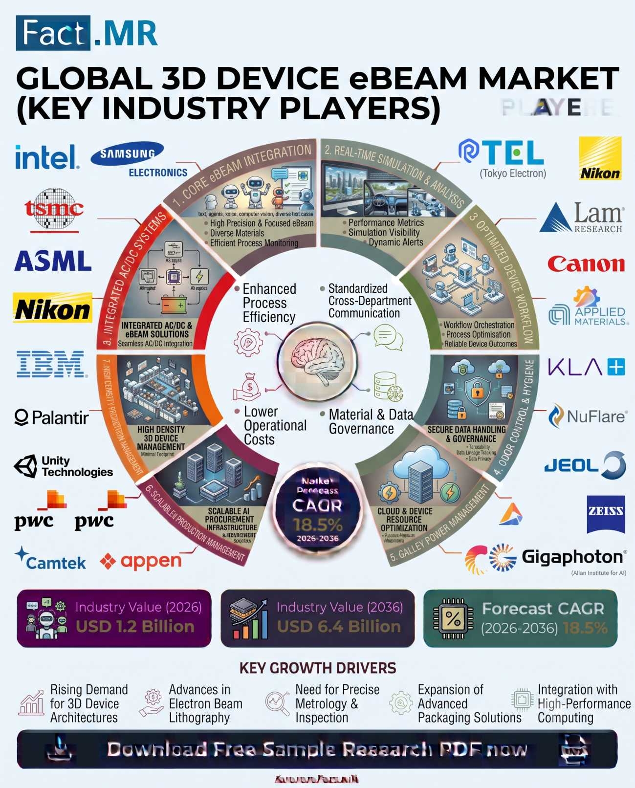
Key companies profiled include ASML (HMI), Applied Materials, Hitachi High-Tech, KLA, JEOL LTD., and ZEISS Semiconductor Manufacturing Technology (ZEISS SMT).
The analysis draws on 120+ sources, 35+ company portfolios, 25+ countries, and more than 20 industry interviews, combining primary research, desk research, market sizing, and data validation.
Contact:
US Sales Office
11140 Rockville Pike
Suite 400
Rockville, MD 20852
United States
Tel: +1 (628) 251-1583, +353-1-4434-232
Email: sales@factmr.com
About Fact.MR
Fact.MR is a global market research and consulting firm, trusted by Fortune 500 companies and emerging businesses for reliable insights and strategic intelligence. With a presence across the U.S., UK, India, and Dubai, we deliver data-driven research and tailored consulting solutions across 30+ industries and 1,000+ markets. Backed by deep expertise and advanced analytics, Fact.MR helps organizations uncover opportunities, reduce risks, and make informed decisions for sustainable growth.