Semiconductor Packaging Market to Surpass USD 55 Billion by 2036 | Fueled by Growing Proliferation of Next-Generation 5G and 6G Networks

0
2KB

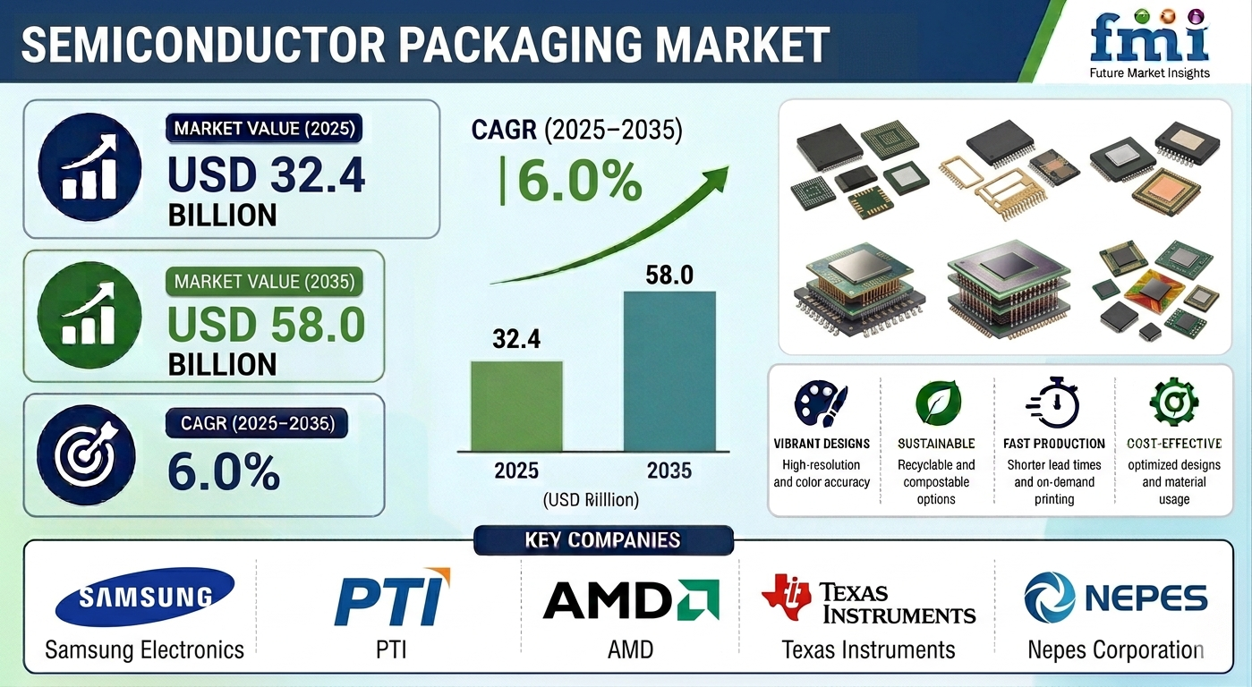
According to Future Market Insights (FMI), The global semiconductor packaging market is witnessing strong growth as demand rises for compact, energy-efficient, and high-performance semiconductor devices across consumer electronics, automotive electronics, AI infrastructure, data centers, and telecommunications applications.

Quick Stats of Semiconductor Packaging Market

  • Market Value (2025): USD 32.4 billion
  • Forecast Value (2035): USD 58.0 billion
  • Forecast CAGR (2025–2035): 6.0%
  • Leading Packaging Type: Grid Array Packaging (41.9% market share)
  • Leading End-use Industry: Consumer Electronics (36.2% share)
  • Fastest Growing Market: United States
  • USA Market CAGR: 6.1%

Get Detailed Market Forecasts, Competitive Benchmarking, and Pricing Trends: https://www.futuremarketinsights.com/reports/sample/rep-gb-15159

Market Overview

The semiconductor packaging industry is rapidly evolving due to growing demand for:

  • AI processors
  • 5G devices
  • IoT systems
  • High-performance computing
  • Automotive electronics
  • Edge computing solutions
  • Cloud infrastructure

Packaging technologies are becoming increasingly important as semiconductor manufacturers focus on:

  • Miniaturization
  • Faster signal transmission
  • Thermal efficiency
  • Power optimization
  • Higher I/O density
  • Compact device architecture

Advanced packaging formats such as:

  • 2.5D packaging
  • 3D IC packaging
  • Fan-out wafer-level packaging (FOWLP)
  • Chiplet integration
  • System-in-package (SiP)

are reshaping the future of semiconductor assembly.

Grid Array Packaging Leads the Market

Grid Array Packaging Holds 41.9% Share

Grid array packaging remains the dominant packaging technology segment due to its:

  • High pin density
  • Excellent thermal performance
  • Strong electrical efficiency
  • Compact footprint
  • High-speed signal capability

Major Grid Array Packaging Formats

  • Ball Grid Array (BGA)
  • Land Grid Array (LGA)
  • Pin Grid Array (PGA)
  • Micro BGA
  • Flip-chip BGA
  • Stacked BGA

These packaging solutions are widely deployed in:

  • Smartphones
  • GPUs
  • AI accelerators
  • Networking processors
  • Memory devices
  • High-performance computing systems

Key Drivers Behind Segment Growth

Advanced grid array technologies offer:

  • Improved heat dissipation
  • Enhanced solder reliability
  • Fine-pitch interconnect support
  • Better signal integrity
  • Higher substrate integration capability

Manufacturers are increasingly integrating:

  • Organic interposers
  • Build-up substrates
  • AI-enabled optical inspection
  • X-ray testing systems
  • Advanced underfill materials

to improve yield performance and long-term reliability.

Consumer Electronics Remains the Largest End-use Segment

Consumer Electronics Holds 36.2% Market Share

Consumer electronics continues dominating semiconductor packaging demand due to massive global production of:

  • Smartphones
  • Tablets
  • Smartwatches
  • Laptops
  • Gaming consoles
  • AR/VR devices
  • Wearables

The push toward:

  • Smaller form factors
  • Better battery efficiency
  • Faster processors
  • Enhanced thermal management

is accelerating adoption of advanced semiconductor packaging technologies.

Key Packaging Technologies Used in Consumer Electronics

  • Wafer-level packaging
  • Chip-scale packaging (CSP)
  • System-in-package (SiP)
  • Multi-chip modules (MCM)
  • Fan-out packaging

Major Industry Trends

Consumer electronics manufacturers are prioritizing:

  • Thin-profile chip packaging
  • High-density interconnects
  • Faster time-to-market
  • Energy-efficient architectures
  • Compact thermal interfaces

The rise of 5G smartphones and AI-enabled edge devices continues driving innovation in semiconductor packaging design.

AI and High-Performance Computing Fuel Market Expansion

The rapid expansion of:

  • Artificial intelligence
  • Machine learning
  • Cloud computing
  • Edge computing
  • Data center infrastructure

is creating significant demand for:

  • High-bandwidth memory (HBM) packaging
  • Chiplet-based packaging
  • 2.5D and 3D stacking
  • Advanced substrate technologies

Semiconductor companies are increasingly investing in heterogeneous integration solutions that combine multiple dies into single advanced packages.

Sustainability and Advanced Materials Gain Importance

Semiconductor packaging manufacturers are increasingly focusing on:

  • Sustainable packaging materials
  • Energy-efficient manufacturing
  • Reduced environmental impact
  • Improved material utilization
  • Lower defect rates

Advanced materials such as:

  • Organic substrates
  • Ceramic packages
  • Encapsulation resins
  • Bonding wires
  • Thermal interface materials

are being optimized for:

  • Higher reliability
  • Better heat management
  • Lower warpage
  • Improved signal transmission

Key Market Drivers

Rising Demand for Miniaturized Electronics

Miniaturization across:

  • Consumer electronics
  • Medical devices
  • Automotive systems
  • IoT products

continues increasing demand for compact semiconductor packaging solutions.

Expansion of AI and 5G Infrastructure

AI chips, edge computing devices, and 5G infrastructure require:

  • High-performance interconnects
  • Faster signal processing
  • Advanced thermal management
  • Dense packaging architectures

This trend is significantly boosting advanced packaging adoption.

Automotive Electronics Growth

The rise of:

  • Electric vehicles (EVs)
  • ADAS systems
  • Autonomous driving technologies
  • Infotainment systems

is creating strong demand for reliable semiconductor packaging with high thermal stability and durability.

Key Challenges

Miniaturization and Thermal Complexity

As semiconductor devices become smaller and more powerful, manufacturers face increasing challenges related to:

  • Heat dissipation
  • Power density
  • Signal integrity
  • Packaging precision
  • Manufacturing complexity

Advanced packaging technologies require expensive infrastructure, skilled labor, and high-precision manufacturing systems.

Semiconductor Supply Chain Constraints

The industry continues facing pressure from:

  • Raw material shortages
  • Substrate supply limitations
  • Geopolitical tensions
  • Fab capacity bottlenecks

which impact packaging lead times and production schedules.

Speak to Analyst: Customize insights for your Business Strategy: https://www.futuremarketinsights.com/customization-available/rep-gb-15159

Country-wise Market Analysis

United States Market Outlook

The USA semiconductor packaging market is projected to grow at a CAGR of 6.1%.

Major Growth Drivers

  • Strong AI infrastructure investment
  • Expanding data center deployments
  • Advanced semiconductor R&D
  • Growing 5G adoption
  • Government semiconductor incentives

The United States continues leading innovation in:

  • High-performance packaging
  • AI-driven chip integration
  • Advanced computing architectures

European Union Market

The European semiconductor packaging market is supported by:

  • European Chips Act initiatives
  • Automotive semiconductor demand
  • Industrial automation growth
  • Supply chain resilience investments

Germany, France, and Italy remain key markets for advanced semiconductor packaging technologies.

United Kingdom Market

The UK market is benefiting from:

  • Growth in IoT devices
  • Advanced substrate R&D
  • Miniaturized packaging demand
  • Edge computing expansion

Government-backed semiconductor initiatives continue supporting local packaging innovation.

Japan Market

Japan remains a strong semiconductor packaging market due to:

  • Robotics manufacturing
  • Precision electronics
  • Sensor technologies
  • High-density interconnect development

Japanese manufacturers are focusing heavily on:

  • Thermal management innovation
  • Chip-scale packaging reliability
  • Advanced substrate engineering

South Korea Market

South Korea continues strengthening its position through:

  • Major memory chip manufacturing
  • HBM packaging investment
  • AI chipset production
  • 3D packaging technologies

Strong integration between packaging and foundry services supports long-term market growth.

Competitive Landsca

Like
1
Rechercher
Commandité
Catégories
Lire la suite
Causes & Effect
Top 7 High-Impact Projects Your Zakat Funded in 2024
Zakat—a pillar of Islam, and a sacred obligation—has the power to do far more than...
Par Ana Flavia Sena 2025-07-31 15:39:24 1 4KB
Non classé
cytotec@Pills In doha (+971569875040)*#Abortion Pills In qatar王al khor王 al wakrah王lusail王 qatar
cytotec@Pills In doha (+971569875040)*#Abortion Pills In qatar王al khor王 al wakrah王lusail王...
Par Alali Mujuba 2025-04-22 15:23:36 0 881
Social Commerce
Experience the Pinnacle of Elegance with 4 BHK Luxury Apartments
4 bhk luxury apartments, In the heart of the modern urban lifestyle, 4 BHK luxury apartments...
Par Saya Avenue 2025-04-22 04:12:11 0 2KB
Social Commerce
Press Release: Crosslinking Agent Market to Witness Growth Acceleration During 2024 – 2030 | +6% CAGR | Exactitude Consultancy
  The latest study released on the global Crosslinking Agent Market evaluates market size,...
Par Amaira Gill 2024-02-21 03:37:12 1 6KB
Social Commerce
BellSouth customer service: A step-by-step guide to get support
Learn how to reach BellSouth email customer service for help with account settings,...
Par Robert Smith 2025-04-21 00:47:58 0 2KB
Talkfever - Growing worldwide https://talkfever.com