

Silicon Wafer CMP Slurry: The Invisible Material That Determines Nanometer Precision Across the Semiconductor Manufacturing Infrastructure
Silicon Wafer CMP Slurry: The Invisible Material That Determines Nanometer Precision Across the Semiconductor Manufacturing Infrastructure
Every advanced semiconductor begins as a polished surface measured not in millimeters but in angstroms. Behind this precision sits Silicon Wafer CMP Slurry, a material that rarely appears in consumer discussions yet influences the performance of processors, memory chips, automotive electronics, AI accelerators, and power devices. As chipmakers push toward smaller nodes, the importance of Silicon Wafer CMP Slurry grows not linearly but exponentially because every reduction in transistor dimensions increases sensitivity to surface defects.
A modern semiconductor fabrication facility may process more than 50,000 wafer starts per month. Each wafer travels through hundreds of manufacturing steps and encounters multiple planarization stages. At advanced nodes, Chemical Mechanical Planarization (CMP) operations can account for 8–12% of total process steps. Within those operations, Silicon Wafer CMP Slurry becomes the functional medium responsible for removing microscopic surface irregularities while preserving structural integrity.
The infrastructure supporting Silicon Wafer CMP Slurry is surprisingly extensive. A leading fabrication facility may consume several hundred thousand liters of slurry annually. Storage systems require contamination control measured in parts per billion. Delivery pipelines, filtration units, recirculation systems, and waste treatment facilities often represent millions of dollars in capital expenditure within a single fab. This means Silicon Wafer CMP Slurry is not merely a consumable; it is an infrastructure component embedded directly into semiconductor manufacturing economics.
The technical challenge solved by Silicon Wafer CMP Slurry is surface planarity. Semiconductor layers are deposited repeatedly during fabrication. Without planarization, uneven topography accumulates after every deposition and etching cycle. Even a surface variation of a few nanometers can create lithography focus issues. CMP processes using Silicon Wafer CMP Slurry routinely reduce surface height variations by more than 90%, creating the flatness required for advanced transistor formation.
The rise of artificial intelligence infrastructure has amplified demand for advanced chips, which indirectly increases dependence on Silicon Wafer CMP Slurry. AI-focused processors contain billions of transistors packed into increasingly smaller geometries. Manufacturing these devices requires tighter defect control than previous generations. Industry engineers often target defect densities below one defect per square centimeter during critical production stages. Achieving such standards is impossible without highly engineered slurry formulations.
A typical Silicon Wafer CMP Slurry formulation contains abrasive particles, chemical additives, pH regulators, oxidizers, corrosion inhibitors, and stabilizers. Abrasive particle sizes frequently range from 20 to 100 nanometers depending on process requirements. Variations of just a few nanometers in particle distribution can alter removal rates significantly. As a result, slurry manufacturing facilities invest heavily in particle characterization systems capable of measuring consistency across millions of particles in each production batch.
The Quantification Story Behind CMP Infrastructure
The semiconductor industry frequently measures productivity through yield. A one-percentage-point yield improvement in a high-volume fab can generate millions of dollars in additional annual output. Silicon Wafer CMP Slurry contributes directly to this equation because surface defects often originate from polishing inconsistencies, particle contamination, or non-uniform material removal.
Consider a fabrication line processing 30,000 wafers monthly. If polishing optimization improves yield from 94% to 95%, annual sellable output may increase by thousands of wafers. This explains why semiconductor manufacturers continuously refine Silicon Wafer CMP Slurry chemistry despite already operating at extremely high precision levels.
CMP infrastructure also demonstrates remarkable water dependence. A single semiconductor fab may consume millions of gallons of ultrapure water daily. During polishing operations, slurry and water interact continuously. Consequently, investments in water recycling infrastructure increasingly influence Silicon Wafer CMP Slurry deployment strategies. Some advanced facilities now target water recovery rates exceeding 80%, reducing both environmental impact and operational costs.
Silicon Wafer CMP Slurry Market Momentum and Forecast Dynamics
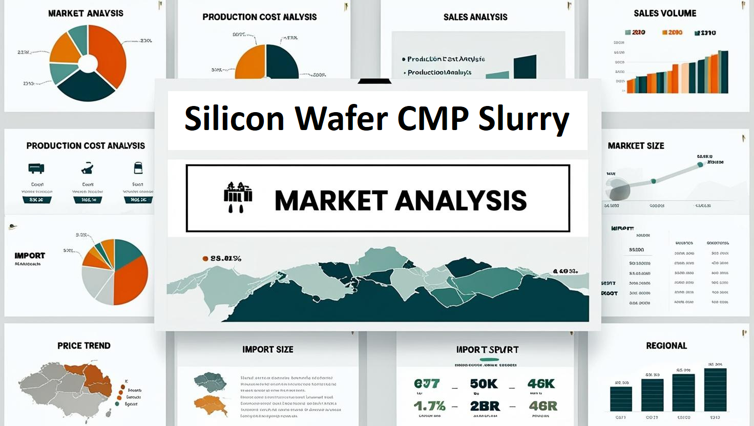
According to Staticker, the Silicon Wafer CMP Slurry market in 2026 is expected to maintain strong momentum driven by advanced logic manufacturing, AI processor expansion, high-bandwidth memory production, and growing automotive semiconductor requirements. The market is projected to register sustained growth through the forecast period as semiconductor fabrication capacity additions continue across Asia-Pacific, North America, and Europe. Staticker attributes future expansion to increasing wafer complexity, rising CMP intensity per wafer, and tighter surface-planarity requirements associated with advanced semiconductor nodes rather than merely higher wafer volumes.
Beyond economics, Silicon Wafer CMP Slurry reflects a broader technological theme: the transition from scaling through transistor count alone to scaling through manufacturing precision. Twenty years ago, many fabrication challenges could be addressed through process redundancy. Today, with features measured in single-digit nanometers, precision itself has become the competitive advantage.
Application Mapping Across Semiconductor Categories
Logic chips represent one of the largest use cases for Silicon Wafer CMP Slurry. Advanced processors often require dozens of polishing stages distributed across transistor formation, dielectric layers, and interconnect structures. Each polishing cycle must maintain uniformity across wafers measuring up to 300 millimeters in diameter.
Memory manufacturing provides another major application. DRAM and NAND architectures continue increasing layer counts and storage density. In advanced memory production, even minor surface deviations can affect stacking reliability. Silicon Wafer CMP Slurry therefore serves as a yield-enabling technology rather than simply a process material.
Power electronics present a different adoption story. Electric vehicles, renewable energy systems, and industrial automation platforms are increasing demand for high-performance semiconductor components. Although manufacturing requirements differ from advanced logic devices, Silicon Wafer CMP Slurry remains essential for achieving consistent wafer surfaces and device reliability.
The automotive sector offers particularly compelling quantification. A premium electric vehicle can contain more than 3,000 semiconductor devices across power management, sensing, infotainment, connectivity, and driver-assistance systems. As vehicle semiconductor content rises, upstream dependence on Silicon Wafer CMP Slurry grows proportionally because every chip requires high-quality wafer preparation before reaching assembly stages.
This creates a powerful infrastructure chain: AI servers increase demand for advanced processors, electric vehicles increase demand for power semiconductors, industrial automation expands sensor deployment, and all three trends elevate the strategic importance of Silicon Wafer CMP Slurry. The material operates far from consumer visibility, yet it influences billions of devices produced annually across the global semiconductor ecosystem.
Request for customization: https://staticker.com/reports/silicon-wafer-cmp-slurry-market/
- Art & Craft
- Causes & Effect
- Dance & Music
- Health & Fitness
- Food & Wellness
- Historic Places
- Homes & Gardening
- Literature & Knowledge
- Science and Technology
- Social Networking
- Social Commerce
- Party & Celebration
- Religion & Festivals
- Shopping & Vendors
- Sports & Games
- Film & Theater
- Digital Creators & Community
- Influencer CCC
- Corporate & Collaboration
- Startup & Scope
- Investment & Growth
- VC & Angel Investors
- Agriculture & farmers
- Nature & Universe
- News & Media
- Real Estate & Property
- Artificial Intellegence
- Political Coverage
- Winners & Loosers
