Looking for platform lift for residential building in delhi? Get platform lift for commercial building in delhi and vertical platform lift in delhi solutions.
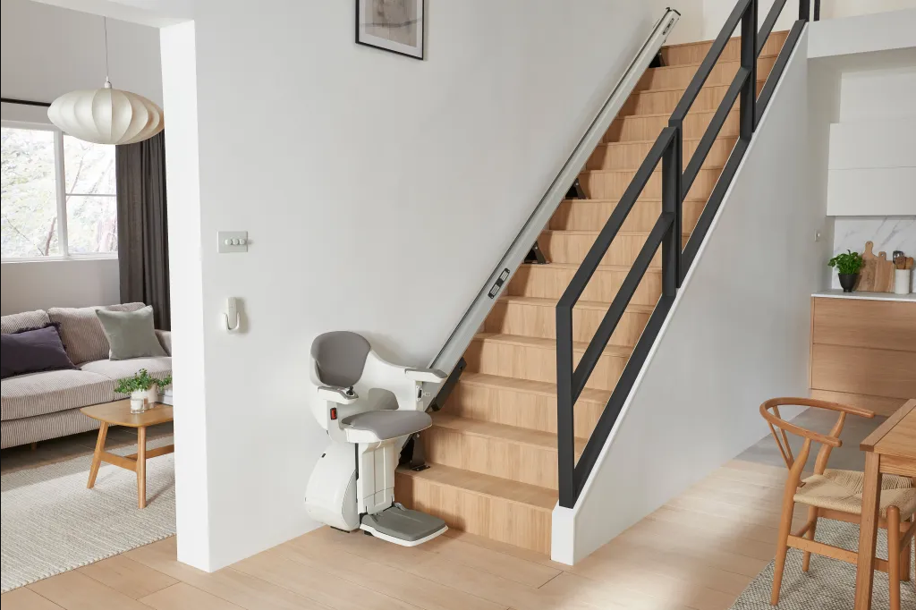
Aristocratic Elevators offers the finest stair lift in delhi and dependable stair lift for senior citizens in delhi for homes, villas, duplexes, and apartments.
Modern buildings are evolving rapidly, and accessibility has become one of the most important aspects of contemporary architecture. Whether it is a luxury villa, commercial office, retail showroom, hospital, or multi-storey residential property, elevators and mobility solutions are now essential for convenience, safety, and comfort. Choosing the right elevator partner plays a major role in...
A 300 mm wafer looks light from outside: nearly 775 square centimeters of silicon, less than 1 mm thick, and often carrying thousands of die positions worth millions of dollars once it reaches advanced process stages. But inside a fab, the problem is not moving the wafer. The problem is holding it flat, centered, thermally stable, particle-safe and repeatable across hundreds of process and...
A semiconductor fab is often described through cleanrooms, lithography tools, etch systems, deposition chambers, and metrology platforms. But behind every 300mm wafer path sits a second industrial layer: machined aluminum plates, stainless-steel vacuum bodies, ceramic fixtures, gas manifolds, wafer-handling arms, precision frames, showerhead plates, heat sinks, chuck interfaces, focus rings,...
A modern semiconductor fab is not only a cleanroom. It is a controlled energy city. A single advanced 300mm fab can operate with electrical load in the range of 80 MW to 150 MW when cleanroom air handling, chillers, vacuum systems, pumps, abatement units, lithography tools, plasma tools, metrology bays, water systems, chemical delivery, and facility automation are counted together. This is why...
A modern chip fab is not only a building with lithography tools, deposition chambers and wafer handlers. It is an air-control machine. A single 300 mm wafer can carry hundreds of dies, and a defect density shift of even 0.01 defects per square centimeter can change the economics of a production lot. This is where ULPA Filter for Semiconductor becomes more than a consumable. It becomes a...
A semiconductor fab is usually described through lithography scanners, cleanrooms, robots, wafers, gases, chemicals, and metrology tools. But beneath that visible architecture sits one of the least glamorous and most quantified infrastructure layers: Semiconductor Vacuum Systems. Every wafer that enters deposition, etch, ion implantation, metallization, inspection, or wafer handling passes...