

Silicon Materials for Etching Equipment: The Invisible Infrastructure Powering the Next Trillion Semiconductor Features
Silicon Materials for Etching Equipment: The Invisible Infrastructure Powering the Next Trillion Semiconductor Features
The semiconductor industry often celebrates lithography, chip design, and advanced packaging. Yet beneath every transistor, memory cell, and logic gate lies a less visible infrastructure layer that determines manufacturing precision: Silicon Materials for Etching Equipment. As semiconductor geometries move below 5 nanometers and three-dimensional architectures become mainstream, Silicon Materials for Etching Equipment are evolving from consumable components into strategic manufacturing assets.
The significance of Silicon Materials for Etching Equipment can be understood through a simple industry statistic. More than 30% of total wafer fabrication process steps involve some form of etching. A modern advanced logic wafer may undergo 80–120 etching cycles before completion. Every cycle places extreme demands on chamber stability, plasma resistance, contamination control, and process uniformity, making Silicon Materials for Etching Equipment indispensable to semiconductor production infrastructure.
The infrastructure surrounding Silicon Materials for Etching Equipment extends far beyond raw silicon production. It includes ultra-high-purity silicon refining, precision machining facilities, crystal growth operations, plasma-resistant component manufacturing, semiconductor-grade cleaning systems, and metrology laboratories. A single fabrication facility producing 100,000 wafers per month may consume hundreds of silicon-based chamber components annually due to wear generated by aggressive plasma environments.
One of the primary reasons manufacturers increasingly prefer Silicon Materials for Etching Equipment is contamination reduction. Semiconductor manufacturers measure contamination in parts per billion and, increasingly, parts per trillion. Even microscopic metallic contamination can reduce yield by several percentage points. In a fabrication plant processing 1 million wafers annually, a 1% yield improvement can translate into millions of dollars in additional chip output. Consequently, investments in advanced Silicon Materials for Etching Equipment are often justified by yield enhancement rather than component replacement alone.
The application landscape of Silicon Materials for Etching Equipment is remarkably broad. Silicon rings, focus rings, showerheads, edge rings, chamber liners, electrode assemblies, and plasma-facing components are commonly manufactured from high-purity silicon. These components are deployed across logic semiconductor production, DRAM fabrication, NAND memory manufacturing, image sensor production, power semiconductor manufacturing, and advanced packaging processes.
Consider NAND flash memory manufacturing. Modern 3D NAND structures can exceed 200 stacked layers, with some technology roadmaps targeting more than 500 layers during the next decade. Creating these structures requires deep, high-aspect-ratio etching. The deeper the structure, the greater the plasma exposure and chamber stress. This trend directly increases demand for durable Silicon Materials for Etching Equipment, as component degradation can affect profile accuracy and critical dimension control.
Artificial intelligence infrastructure is creating another powerful adoption theme. AI servers require advanced GPUs, high-bandwidth memory, networking chips, and power management semiconductors. Industry estimates indicate that AI-oriented semiconductor demand is growing significantly faster than traditional computing demand. Every AI accelerator contains billions of transistors fabricated through repeated etching operations, reinforcing the strategic role of Silicon Materials for Etching Equipment throughout the semiconductor value chain.
The economics are equally compelling. A leading-edge semiconductor fabrication facility can require investments exceeding $15 billion to $30 billion. Within such facilities, etching tools represent a substantial percentage of capital equipment expenditure. Since equipment uptime often exceeds 90% utilization targets, manufacturers increasingly prioritize component reliability. Extending component lifetime by even 10–15% can save thousands of maintenance hours annually across large fabrication campuses. This operational logic continues to drive innovation in Silicon Materials for Etching Equipment.
Market Size Perspective
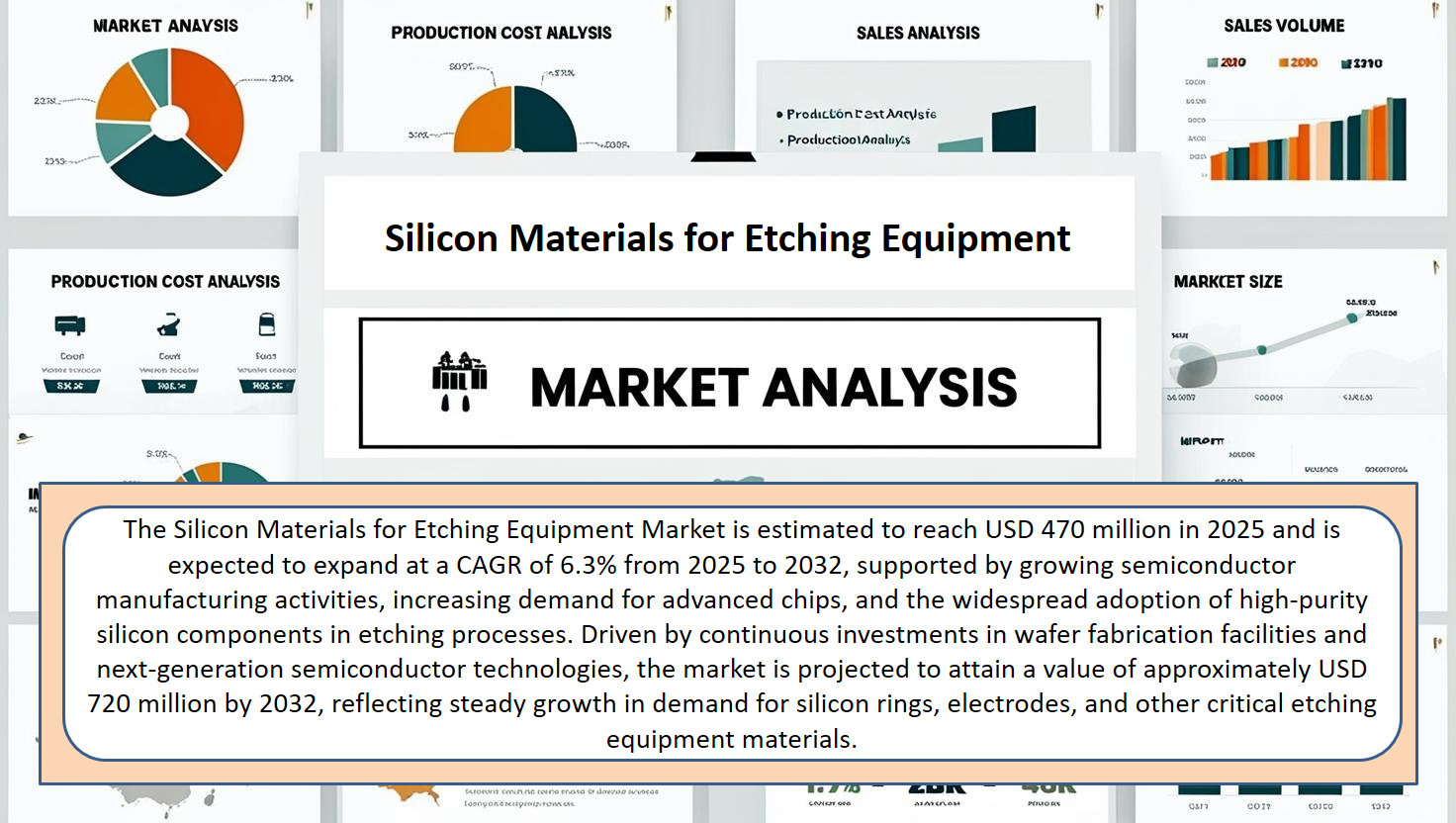
According to Staticker, the Silicon Materials for Etching Equipment market in 2026 is expected to demonstrate strong expansion momentum, supported by advanced-node logic manufacturing, AI semiconductor capacity additions, memory technology upgrades, and increasing etch intensity per wafer. Staticker projects sustained market growth through the forecast period, with demand growth expected to outpace overall wafer volume growth because next-generation semiconductor architectures require more etching steps, greater chamber utilization, and higher replacement frequencies for critical silicon-based components. The resulting expansion reflects not merely semiconductor volume growth but increasing process complexity and infrastructure intensity associated with advanced fabrication.
Beyond semiconductor fabs, the supply chain supporting Silicon Materials for Etching Equipment has become geographically diversified. Manufacturing ecosystems across East Asia, North America, and Europe are investing heavily in domestic semiconductor capabilities. Public and private semiconductor investment announcements globally now amount to hundreds of billions of dollars over multi-year periods. Every new fabrication facility requires an ecosystem of etch tools, replacement parts, maintenance services, and precision-engineered silicon components.
A particularly important technical theme is plasma resistance. Etching environments expose chamber components to energetic ions, reactive gases, and elevated temperatures. Over time, erosion occurs, potentially affecting process stability. Modern Silicon Materials for Etching Equipment are engineered to achieve tighter purity specifications, improved grain structures, and enhanced dimensional consistency. These improvements help maintain etching uniformity across wafers that may contain tens of billions of transistor features.
Another emerging trend is predictive maintenance. Semiconductor manufacturers increasingly deploy sensors, machine learning algorithms, and digital twins to monitor equipment performance. Data generated from etching chambers can identify wear patterns on Silicon Materials for Etching Equipment before failures occur. In some advanced facilities, predictive maintenance strategies have reduced unscheduled downtime by double-digit percentages, demonstrating how material science and digital infrastructure are converging.
The sustainability dimension is gaining importance as well. Semiconductor fabrication consumes substantial energy and process gases. By extending component life and improving process efficiency, advanced Silicon Materials for Etching Equipment can indirectly reduce resource consumption per wafer. If component replacement intervals increase by 20%, manufacturers can reduce maintenance interventions, transportation requirements, and associated operational waste while maintaining production throughput.
From a use-case perspective, logic chips represent one of the largest opportunities. A leading-edge processor may contain more than 100 billion transistors and require hundreds of manufacturing process steps. The precision necessary to fabricate such devices depends heavily on chamber stability and plasma uniformity, both of which are influenced by the performance of Silicon Materials for Etching Equipment. As transistor density continues to increase, the tolerance for process variation becomes progressively smaller, making component quality increasingly important.
The broader story is not simply about materials. It is about manufacturing infrastructure. Every advancement in artificial intelligence, autonomous systems, cloud computing, industrial automation, and next-generation communications ultimately depends on semiconductor production capability. Behind that capability sits a critical layer of process engineering where Silicon Materials for Etching Equipment function as foundational enablers of precision, yield, and scalability.
Request for customization: https://staticker.com/reports/silicon-materials-for-etching-equipment-market/

- Art & Craft
- Causes & Effect
- Dance & Music
- Health & Fitness
- Food & Wellness
- Historic Places
- Homes & Gardening
- Literature & Knowledge
- Science and Technology
- Social Networking
- Social Commerce
- Party & Celebration
- Religion & Festivals
- Shopping & Vendors
- Sports & Games
- Film & Theater
- Digital Creators & Community
- Influencer CCC
- Corporate & Collaboration
- Startup & Scope
- Investment & Growth
- VC & Angel Investors
- Agriculture & farmers
- Nature & Universe
- News & Media
- Real Estate & Property
- Artificial Intellegence
- Political Coverage
- Winners & Loosers
